Is DC-DC VRM really a good design?
작성자: FSP Group
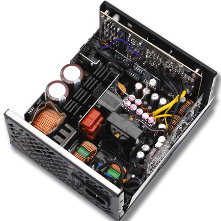
Amid the fast growing developments in the gaming industry, game players are placing increasing demands on computer components which, in turn, lead to more supplier efforts in pursuing still better performance. This is especially the case with power supply, the very core of every computer, as it is the source of power in driving each and every computer component. This is the reason why individual professional product evaluation media and reviewers are focusing on products with DC-DC VRM design for secondary side outputs of advanced computer power supply for more reliable power outputs.
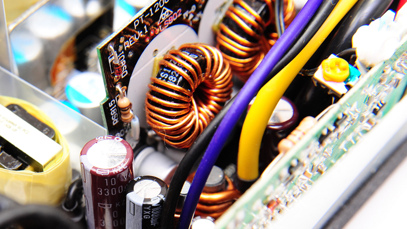
Let’s review the direct current to direct current voltage regulation module (DC-DC VRM) first. As its name suggests, the DC-DC VRM is a power conversion module for DC input to DC output with little voltage variations in between. The DC-DC VRM design features good power conversion efficiency at 95% or better, excellent output voltage steadiness and better than conventional magnetic amplifier’s ripple noise. All these contribute towards providing advanced game players with these power supplies.
In addition to these benefits, the DC-DC VRM design is being adopted lately by advanced products for two other reasons, although admittedly at higher costs. The one is the unstable voltage of multiple unbalanced load outputs by conventional power supply and the other is the failure of the main +12V output in meeting the total rated power of the entire power supply.
You may not be clear about unstable unbalanced load outputs by a conventional magnetic amplification circuit. The seesaw phenomenon dreaded by power engineers may come true along with higher +12V and lower +3.3V or +5V loads. In a multi-output power circuit without feedback design voltage at the +12V end may get even higher while the +3.3V or +5V will be lower and eventually end up with the reliability falling out of the acceptable range of computer components. This is not the case with power the supply using the DC-DC VRM design.
As input of the +3.3V or +5V circuit is provided by the +12V output of the main power conversion circuit, the former is actually a load of the latter. This mandates the power conversion design of the +12V circuit to level the rated power of the entire source. This means that when less power is required at the +3.3V or +5V circuit, there can be more juice available to the +12V circuit compared with its conventional magnetic amplification circuit counterpart. No wonder high end gamers prefer products with these designs.
However, this does not mean a death sentence for the power supplies of conventional magnetic amplification circuit designs. The power supply specifications set forth by Intel have defined the variation range of voltage output (see Keys in Choosing a Power Supply) which power supply manufacturers are required to comply with. The test and inspection mechanism of this requirement, the Cross Load Regulation, has also been adopted by each manufacturer. Game players need not worry too much about the high costs of DC-DC VRM design as long as less than perfect performance of certain items is not your concern.
Related Post: AC/DC Power Supply Design in 7 Steps


관련 기사


FSP소개
세계 최고의 전원공급장치 제조업체인 FSP그룹은 1993년 설립 이래 '서비스, 전문, 혁신'이라는 경영 철학을 바탕으로 포괄적인 그린 에너지 솔루션 제품을 공급하고 있습니다.