AC/DC Power Supply Design in 7 Steps
Overviews
- What is an AC-DC Power Supply?
- Should I Design and Make, or Just Buy It?
- AC/DC Power Supply Design Process
- Step 1: Plan & Define Basic Electrical Properties Characteristic
- Step 2: Complete the PCB layout
- Step 3: Sampling
- Step 4: Weld the components in the BOM list onto the PCB
- Step 5: Electronic property verification and adjustment
- Step 6: Trial Production and Re-verification
- Step 7: Obtain Safety Certification to Sell Locally
- FSP Group AC-DC Power Supply Recommendations
- Conclusion
What is an AC-DC Power Supply?
An AC-DC power supply is a device that converts alternating current (AC) to direct current (DC). This conversion is necessary for many electronic devices, as most require stable DC voltage to operate, such as the external transformers used with laptops, media players, gaming consoles, and almost all consumer and industrial electronic products. The conversion process typically involves the following steps: transformation, rectification, filtering, and regulation.
Working Principle
- Transformation: First, the AC power passes through a transformer to lower the voltage to the desired range. The primary coil of the transformer is connected to the AC power source, and the secondary coil outputs the transformed AC voltage.
- Rectification: The transformed AC voltage then passes through a rectification circuit (usually a diode bridge rectifier) to convert the AC to pulsating DC.
- Filtering: The pulsating DC is smoothed by a filter (typically using capacitors and inductors) to remove the pulsations, resulting in a smoother DC voltage.
- Regulation: Finally, a regulator adjusts the DC voltage to ensure a stable output voltage, regardless of variations in input voltage or load.
Applications and Types
AC-DC power supplies are widely used in various electronic devices, including household appliances, computers, communication equipment, medical devices, industrial control systems, and more. Depending on application needs, AC-DC power supplies come in various designs and configurations:
- Linear Power Supply: Based on transformers and linear regulators, these power supplies are bulkier but offer stable and low-noise output. Due to low efficiency and high heat dissipation, they are mostly used in high-noise-sensitive audio systems.
- Switching Power Supply: Also known as switch-mode power supplies, these use high-frequency switching technology, offering high efficiency and compact size, making them suitable for a wide range of applications. These power supplies provide higher power in smaller sizes and are currently the mainstream product on the market.
Ever since Nikola Tesla won the current war and established the alternate current (AC) type as the transmission and distribution system, power supplies featuring the conversion of AC high voltage into direct current (DC) low-voltage intended for electronic components have been in existence. Up to the present, power supplies have been developed from bulky linear transformers at first into various switching power supplies with various topologies. In addition to their reduced sizes, they have become more efficient and reliable.
The output power of a conventional linear transformer power supply is proportional to its volume and weight. A linear transformer of about 10W weighs approximately 300g, but if the out power is increased to 100W, its weight will increase by multiple folds to around 3~5kg. Even moving it around at home is like weight training, let alone bringing it during travel. Not only that, if the basic voltage feedback feature is required, but a linear regulator also needs to be installed. This regulator consumes the voltage, which exceeds the specification through heat loss. Therefore, in order to reasonably control temperature rises, a large heat sink needs to be installed, which makes the whole power supply larger, thus its doubled weight. That said, other than some audiophiles that have extremely high standards for ripple noise, there is almost no demand for linear power supplies.
Currently, there are many application scenes and categories of power supplies. In addition to homes and offices familiar to us, there are specific needs in certain application scenes, such as medical care, heavy industry, automobiles, laboratory equipment, data centers, 5G applications, railways, navigation, and so on. At the same time, in response to different applications power supplies whose electrical property, appearance, weather resistance, and redundancy meet specific tasks have been developed.
AC/DC Power Supply: Should I Design and Make, or Just Buy It?
What does it take to design a good power supply in different application scenarios? With the adaptor power supply most commonly used in notebook computers (NBs) as the example below, let us see how an adaptor for NBs is designed to be competent for tasks assigned. Let us also compare whether to buy a finished product or attempt to design it and make a product of our own.
Below listed the process when designing AC to DC power supplies:
- Plan & define basic electrical properties characteristic
- Complete the PCB layout
- Sampling
- Weld the components in the BOM list onto the PCB
- Electronic property verification and adjustment
- Trial production and re-verification
- Obtain safety certification to sell locally
We’ll take a 120w adaptor for NBs for example, to explain how to design AC to DC power supplies step by step.
AC/DC Power Supply Design Process
Step 1: Plan & Define Basic Electrical Properties Characteristic
Generally speaking, during the early part of a power supply design, the basic electrical properties characteristic should be first defined. Below, a 120W adaptor for NBs is used as an example to take a view of the items to be defined and the general parameters. They include input voltage and frequency, appearance and dimensions, operating temperature and humidity, input AC socket, overall efficiency, standby power consumption, output voltage, output current, peak load, protection (including OCP/OVP/OTP), various EMC needs, etc.
The above are tabulated below to make them clear and easy to understand.
|
Item |
Specifications |
|---|---|
|
Input voltage and frequency |
90 ~264Vac (50/60Hz) |
|
Appearance and dimensions |
123*45*67 mm |
|
Operating temperature and humidity |
-10℃ ~ 40℃ |
|
Input AC socket |
C14 |
|
Output voltage |
19V±5% |
|
Output current |
6.3A |
|
Overall efficiency |
Follow DoE level VI & CoC Ver. 5 tier2 |
|
Standby power consumption |
0.15W |
|
Peak Load |
x 2 (50mS@1sec period) |
|
Protection (including OCP/OVP/OTP) |
Latch / hiccup |
|
Various EMC needs |
IEC62368-1 |
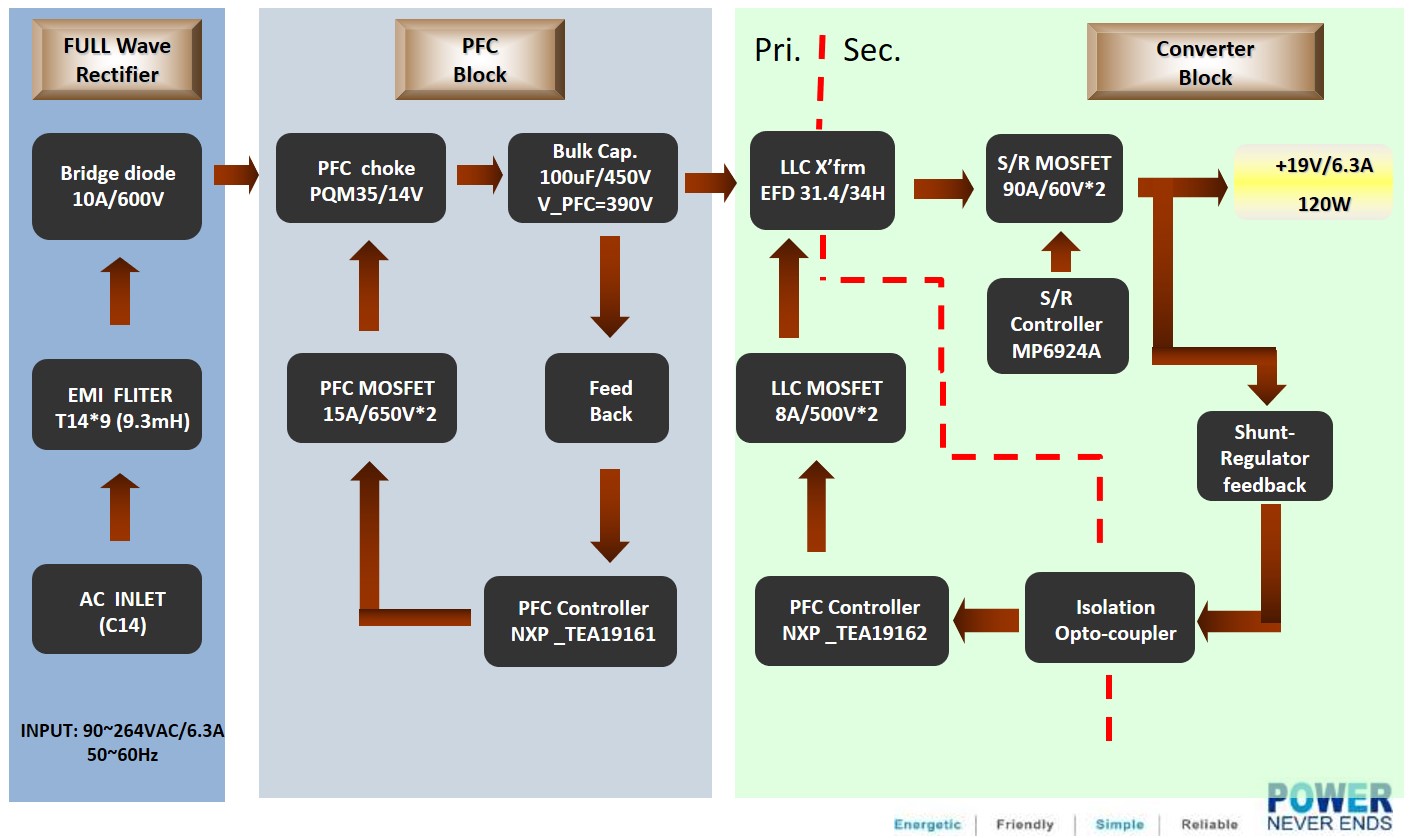
After roughly determining the electrical characteristic, it was time to select an appropriate topology. For a 120W adapter, topologies available for selection generally include Flyback, ACF (active-clamp flyback), and HB-LLC. That said, in view of the increasingly stringent regulatory requirements, Flyback characterized by excessively low efficiency may not be suitable. Although the rest (ACF and HB-LLC) are accomplishable, considering it is more difficult to adjust ACF’s light load efficiency, HB-LLC was selected as the topology this time.
After selecting the topology, in order to ensure a smooth design process, a block diagram is usually opted. The circuit structures of different blocks and the names of the main IC or components selected are roughly distinguished first. Moreover, in consideration of the input power of >75W, In line with the EU’s total harmonic distortion requirements, a PFC circuit should be added to meet the EU requirements.
The diagram below is the block diagram drawn according to the above-mentioned electrical characteristic and in accordance with the appropriate components based on the HB-LLC structure.
So far, with the planning phase still ongoing, designers familiar with the power supply structure may not show obvious differences in terms of their choice between buying a finished product or designing it by themselves. However, the difference between the two gradually becomes clear when subsequently entering the implementation phase.
Step 2: Complete the PCB layout
In general, the PCB layout phase follows after confirming the circuit structure and selecting the components. As for how to place all the components to fit the specifications specified by customers while taking into account the electrical characteristic and safety distance, reducing production and assembly difficulties, production automation, thermal convection, and other conditions, it will take a professional layout engineer and suitable software to do the job. Take this 120W adaptor, for instance, it will take an experienced layout engineer about a week to complete the first edition of PCB from scratch.
Step 3: Sampling
The completed PCB file will then be sent to the PCB vendor specialized in sampling to schedule a sample production. It normally takes about 3~5 working days at USD200 sampling charges to obtain 10~15 pieces of PCB samples. To cut down costs, players engaging in self-design may, of course, attempt to perform etching and washing using a PCB bare board with copper foil they have purchased. Nevertheless, considering there is low precision, copper wire breaks easily, and the finished product only has the copper foil layer (See Figure 1 below) without the upper/lower layer silk screen (See Figures 2&3) as an assembly reference, not to mention the need to purchase a bunch of chemical etching liquids and the challenge of accurately drill holes on the PCB one by one. Under the circumstances that not much money is saved and that failure rates are high, the self-production of PCB is not recommended.
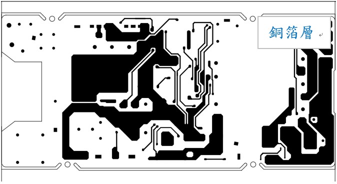
Figure 1: copper foil layer
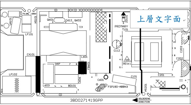
Figure 2 : upper layer silk screen
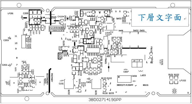
Figure 3: lower layer silk screen
Step 4: Weld the components in the BOM list onto the PCB
Once the PCB is completed, all the components in the BOM list prepared in the early stage are manually welded onto the PCB. In general, the assembly sequence is SMD first followed by DIP. Assemble small components first and then large components. This way, assembly interference and missing components in the assembly are less likely to result. However, a manual assembly cannot be completely free of errors. Moreover, since multiple prototypes are assembled manually, problems occurring in each prototype may vary. Missing parts, misalignment, reverse polarity, and so on all add to the difficulty of prototypes. Eventually, it will take at least a week from sampling to start-up, not yet including the material preparation time in the early stage of all the components in the BOM list. At this stage, if self-design players only produce one prototype, it will take less time, provided the material preparation time and cost in the early stage are not included in the calculation. Since individual players have limited access to resources, they must purchase all the components one by one to an electronic material store. Preparing all the materials for one prototype is definitely 2~3 times as costly as buying a finished power supply product.
Step 5: Electronic property verification and adjustment
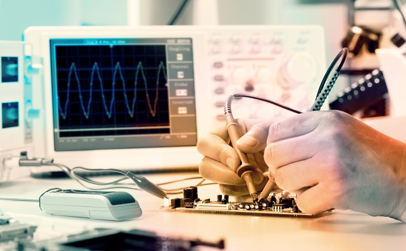
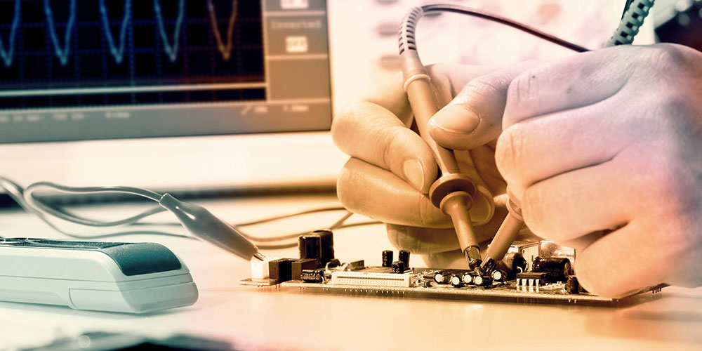
After completing the start-up steps, the electronic property verification and adjustment phase follows. In order to simulate power the systems of different countries and various load conditions, many related instruments and devices are needed to complete electronic property verification, including programmable AC power supplies and analog electronic dummy loads. Of course, high-precision oscilloscopes and related probes (voltage probes/current probes/differential probes), digital meters, power meters, and temperature-controlled soldering irons are essential as well. Under certain situations, small signals on circuits need to be confirmed. In that case, a DC power supply is a necessary gear. That said, the above instruments will not be something the average player can afford. To advance further, a set of frequency response analyzer worth NTD1 million is also a necessary gear to achieve high feedback stability and adequate phase margin and gain margin.
If you still have not switched the channel thus far, you sure have a passion for power supplies! To live up to your studious spirit, let us continue…
In terms of the first edition of samples, R&D personnel generally perform verifications related to the basic electrical characteristic, temperature rises, EMI, and EMS. However, since power supplies are categorized under analog circuits, oftentimes, a certain electrical modification countermeasure may bring about side effects. This will cause another electrical property or verification item to exceed specifications, which may have a ripple effect and time and bring challenges to developers over and over again (this phenomenon is known as the seesaw effect in which the supposedly passed parameter B fails again after the countermeasure of Parameter A is modified. Hence, how to properly handle the situation will rely on meticulous adjustments by an experienced engineer). Hence, in addition to a preliminary test by R&D personnel, the FSP has set up a full-time verification department to conduct verification one by one from a third-party perspective. This will, in turn, ensure product quality.
The table below shows FSP’s normal power supply items that require verification.
QUALIFICATION TEST REPORT
| Customer: | Moder name: FSP120-AAAN3 | Tested by: XXX |
| Report Rev: 01 | Stage: B-TEST | Checked by: XXX |
| Spec. Rev: 1.00 | Date: XXX | Approved by: XXX |
| S/N: S7510030032 |
| Item | Sub-Item | Results | Page | Comments |
|---|---|---|---|---|
|
Input Characteristics |
Efficiency | Pass | 1-3 | |
| Input current | Pass | 1-2 | ||
| Power factor | Pass | 1-2 | ||
| Inrush current | Pass | 4 | ||
| Turn on time | Ref. | 24 | ||
| Hold up time | Pass | 25 | ||
|
Output Characteristics |
Output voltage regulation | Pass | 5-6 | |
| Ripple & Noise | Pass | 7-8 | ||
| Dynamic load | Pass | 9-13 | ||
| Overshoot | Pass | 14-18 | ||
| P.G delay timing | Pass | 26 | ||
| P.G fail timing | Pass | 27 | ||
| Raise time | Pass | 28 | ||
|
Protections |
Short circuit | Pass | 19-20 | |
| Over current | Pass | 21 | ||
| Over voltage | Pass | 22-23 | ||
|
Safety |
Leakage current | Pass | 37 | |
| Hi-pot | Pass | 38 | ||
| Insulation resistance | Pass | 39 | ||
| Ground bond | Pass | 40 | IEC60068-2-2 | |
|
Environment/Reliability |
Thermal | Pass | 32-36 | |
| Burn in | Pass | 41 | ||
| Acoustic emissions | Pass | 53-55 | ||
| ON/OFF cycling | Pass | 56 | ||
| Low temperature storage | Pass | 57 | IEC60068-2-1 | |
| High temperature storage | Pass | 58 | IEC60068-2-2 | |
| Temperature & Humidity cycling | Pass | 59 | IEC60068-2-14 | |
| Cold start | Pass | 60 | IEC60068-2-1 | |
| Voltage stress | Pass | 61-74 | ||
| Vibration | Pass | 75-77 | IEC60068-2-64 | |
|
E.M.C. |
Current harmonic | Pass | 29-31 | EN61000-3-2 |
| Lighting surge | Pass | 42-43 | EN61000-4-5 | |
| ESD | Pass | 44-45 | EN61000-4-2 | |
| EFT | Pass | 46-47 | EN61000-4-4 | |
| EMI conduction | Pass | 48-52 | EN55032 | |
| AC voltage dips | Pass | 78-79 | EN61000-4-11 |
Self-design players generally lack complete test instruments and devices. Therefore, after turning on the first edition of samples, they can only use a simple multi-meter to verify the voltage correctness. In better scenarios, the self-design players may come with load resistance that can be applied for basic aging and temperature rise tests. However, without more sophisticated devices, more difficult problems may be encountered, which will get players stuck and make further verification impossible. Even with normal turn-on, stability and lifespan remain uncertain. Having said that, if all the processes work out and problems get solved, it is worth the while being able to independently complete a power supply even though it may be more costly than directly buying a commercially available power supply. After all, the sense of achievement is priceless.
Having said that, self-designed power supplies are at a higher risk and are not recommended for use on more pricey products. In case something goes wrong at work, the power supply may fail; in severe cases, the backend electrical appliances will be damaged, which is more a loss than gain. At this point, this will probably be it for general self-designed power supplies, but each of FSP’s qualified power supplies will still need to go through the following stages.
Step 6: Trial Production and Re-verification
After the electrical properties are initially verified by R&D personnel, trial production will be arranged at the factory. This is done in the hopes of finding areas of production difficulty before officially commencing mass production. This will reduce defect rates during mass production. On the other hand, since trial production samples are more complete than manually-operated samples and are larger in quantity, the FSP’s verification department will use the samples to perform verification. In addition to the items verified by the above-mentioned R&D personnel, additional components derating and open short verifications are also done. Components derating is mainly intended to determine if the surplus of all the components is in line with the specifications of the components during power operation. If there is an excess, it will be brought up for the R&D personnel to make improvements. Open short is mainly intended to verify what reactions arise from the power supply when a component fails or the open circuit or short circuit phenomenon occurs in a single unit. Since power supplies are connected to mains, in theory, energy is inexhaustible. If the power supply fails, causing the generation of heat, smoke, or even sparks, it may result in major safety accidents. Such outcomes are completely unacceptable. Therefore, open short simulates all possible adverse results to exclude possible dangers before they take place. Because the two above-mentioned tests are intended to verify every component of the power supply, verification is highly time-consuming. Additionally, simulating the open short status often damages the power supply. Thus, numerous samples are required, which cannot be completed by R&D personnel alone but by a dedicated verification unit.
Step 7: Obtain Safety Certification to Sell Locally
As mentioned in the contents above, when the power supply fails, major safety concerns may arise. Power supplies may also have different safety considerations when used in different venues. Although many international organizations such as the IEEE(Institute of Electrical and Electronics Engineers) have set up recommended specifications, considering the differed mains voltages of different countries, the AC socket and the definition of safety varies from country to country. In the end, the countries around the world have developed their own sets of criteria. This way, adaptors for NBs possibly sold and used by any country in the world will have to be tested through the assistance of a professional laboratory and in accordance with the requirements of the country it is in. Finally, a safety certification from the country must be obtained for products to be allowed to be sold locally, and that is just one country. If universal use is to be taken into consideration, we will need to apply for a safety certification from each country one by one. Most certainly, this will cost a considerable amount of money. On top of it, such a safety certification is a mandatory requirement with legal binding power. Non-compliance will result in fines and the product no longer being sold.
FSP Group AC-DC Power Supply Recommendations
FSP Group is a leading global manufacturer of power supplies, with extensive industry experience. Since its founding in 1993, it formed a strategic alliance with Intel to successfully develop the ATX series products. Today, its product line has expanded to UPS systems and power supply products for various niche markets, providing ODM and OEM services for enterprises. FSP’s products are customer-oriented, adhering to various ISO standards, and promoting its own quality assurance and safety standards (PCDA). The company has built a strong reputation for innovation in the market. For example, its open frame power supply products for electrical equipment offer the following specifications and features (details available at the link):
- Customizable - Open frame power supplies can be easily installed in any convenient and safe location within electrical device enclosures.
- Various Form Factors - FSP manufactures open frame power supplies in 2x4 inch and 3x5 inch sizes. We can also design and manufacture open frame power supplies according to special designs and specifications.
- Wattage and Voltage - FSP’s open frame power supplies offer options from 30W to 450W and output voltages from 5V to 54V (including 12V+54V).
Know more: FSP Open Frame Power Supply Products
Industrial Computer Power Products:
- Compliant with IEC 62368 and IEC 60950 safety standards
- Capable of handling extreme temperatures with high MTBF (Mean Time Between Failures) ratings
- 80 Plus Gold and Platinum certified
- Wattages ranging from 100W to 3,000W. Our industrial computer power supplies also offer various input voltage options, including 115V AC, 230V AC, LVDC, and HVDC.
Know more: FSP IPC Power Products
Conclusion
At this time, the main stages from scratch of a qualified power supply can be depicted. Of course, many details cannot be described in detail. The numerous waveforms and test data confirmations, alternative material verifications, special regulations, specific environment requirements, new material adjustments, etc. add insurmountable unknowns to the difficulty involved in power design.
Returning to the issue of individually designed power supplies, in addition to their higher costs compared to commercially available power sources, personal efforts in specification formulation/circuit structure IC selection/transformer model selection/winding design/circuit drawing/PCB layout/material procurement/prototype assembly/and finally debugging of electrical properties will not only cost money but will also require a great deal of time and energy to complete the whole process. In addition to personal competency, considerable enthusiasm is needed, not to mention the lack of ability to afford costly instruments and devices to perform electrical property verifications and complicated quality verification processes. This will, in turn, result in the high unreliability of finished products.
Clearly, power supply DIY that comes with a low cost-performance ratio is not such a great idea after all. It might just as well be a challenge for students or self-fulfillers to take on.
Related articles:<How to Choose a Power Supply? AC-DC Power Supply Introduction>


Related Articles
-

Differences between designing an industrial power supply and a personal power supply
-

Comprehensive Guide to Industrial PC (IPC) Power Supplies: Common Applications, IEC61000 EMC Standards, and Key Selection Criteria
-

How to Choose a Power Supply? AC to DC Power Supply Introduction
-
How to Select AC-DC Power Supply for Peak Load Requirement
About FSP
FSP Group is one of the global leading power supply manufacturer. Since 1993, FSP Group has followed the management conception “service, profession, and innovation” to fulfill its responsibilities as a green energy resolution supplier.